Monday, September 16
Device Testing Invited Talk - CDM Bare Die Testing, ESDA CDM Joint Working Group Technical Report Overview
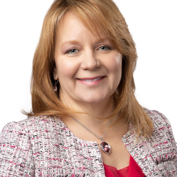
Kathleen Muhonen
Kathleen Muhonen is currently an ESD engineer at Qorvo in Greensboro, NC. She is involved in ESD on-chip protection for RF and Millimeter wave applications. She is heavily involved in system level testing that helps standardize IED testing of RF components and instrumentation for better ESD characterization of clamps and materials. Previously she was responsible for RF characterization and model support for SOI switches and Gallium Arsenide power amplifiers. She has also done extensive work on developing state of the art harmonic and breakdown characterization system for semiconductors and has improved de-embedding techniques of large-scale modeling structures. Kathleen's previous experience includes assistant professor at Penn State Erie, linearization design for base stations at Hewlett Packard, and power amplifier design at Lockheed Martin and GE Aerospace.
Kathleen is a member of the ESD association and is on all device testing standards committees, including serving as past TLP and HMM workgroup chairs. She has also served on the Board of Directors and is now serving as the education committee chair. Kathleen received her BSEE degree from Michigan Technological University in 91, a MSEE from Syracuse in 94 and a PH.D.EE from Penn State University in 99.
Device Testing Invited Talk - CDM Bare Die Testing, ESDA CDM Joint Working Group Technical Report Overview
1B.1 TLP/VFTLP Investigation on eNVM 1T1R PCM in FD-SOI UTBB CMOS Technology at Room Temperature (ESREF Invited Paper)
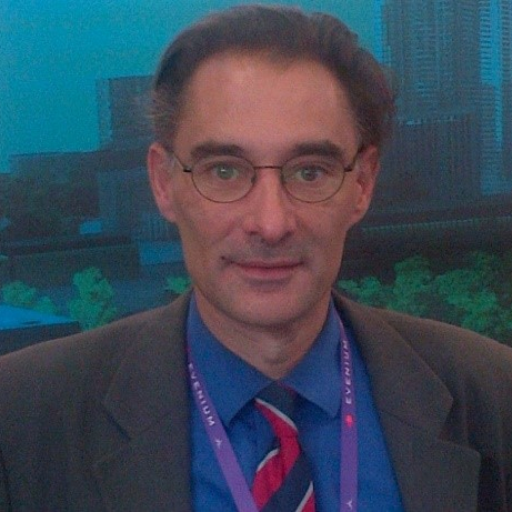
Philippe Galy
Dr. Philippe Galy, born 1965, obtained his Ph.D. from the University of Bordeaux (France) in 1994. He holds also a H.D.R. (academic research supervisor) from LAAS CNRS University of Toulouse in 2005. He has authored or co-authored over 150 publications, 4 books, and 140 patents portfolio. Philippe serves in several technical program committee and he is a reviewer for many symposiums and journals (Ex: Nature/VLSI/TED/TON/SSE/ ESREF/ESSDERC/ICICDT/EUROSOI/CAS).
He joined STMicroelectronics in 2005, working on ESD/LU and new solutions from device to SOC level in advanced CMOS and mature technologies (Bulk / FD-SOI / planar & 3D). He develops tooling concepts for robust IP integration and supervises its developments till massive production. Moreover, its main R&D topics are on SCR, T2, TFET, BIMOS transistor, Beta-structure and other innovative devices for emerging neuromorphic, Qubit applications. Philippe is in charge for STMicroelectronics on Cryogenic Quantum R&D with many international partners. Based on these topics he supervises 16 PhD. He was already involved in National & European projects ( Ex.: Nano 2017/ROBIN/REMINDER/Neuram3/ QLSI/ARCTIC). Also, he joins the QuEng CDP group from Grenoble France. Its Position today is Fellow technical Director and adjunct professor at UdS.
1B.1 TLP/VFTLP Investigation on eNVM 1T1R PCM in FD-SOI UTBB CMOS Technology at Room Temperature (ESREF Invited Paper)
1B.2 Can CC-TLP be used as an Early Failure Analysis Tool?
Chloe Troussier
Chloé Troussier received her Ph.D. degree in 2022 from University Grenoble Alpes of Grenoble, France. During her Ph.D. thesis (20018-2022), she worked on on the study of Charged Device Model phenomenon in STMicroelectronics. Since 2021, she joined STMicroelectronics Crolles as a Research Engineer working on ESD protections and strategies.
1B.2 Can CC-TLP be used as an Early Failure Analysis Tool?
Authors Corner for 1B.1 and 1B.2

Philippe Galy
Dr. Philippe Galy, born 1965, obtained his Ph.D. from the University of Bordeaux (France) in 1994. He holds also a H.D.R. (academic research supervisor) from LAAS CNRS University of Toulouse in 2005. He has authored or co-authored over 150 publications, 4 books, and 140 patents portfolio. Philippe serves in several technical program committee and he is a reviewer for many symposiums and journals (Ex: Nature/VLSI/TED/TON/SSE/ ESREF/ESSDERC/ICICDT/EUROSOI/CAS).
He joined STMicroelectronics in 2005, working on ESD/LU and new solutions from device to SOC level in advanced CMOS and mature technologies (Bulk / FD-SOI / planar & 3D). He develops tooling concepts for robust IP integration and supervises its developments till massive production. Moreover, its main R&D topics are on SCR, T2, TFET, BIMOS transistor, Beta-structure and other innovative devices for emerging neuromorphic, Qubit applications. Philippe is in charge for STMicroelectronics on Cryogenic Quantum R&D with many international partners. Based on these topics he supervises 16 PhD. He was already involved in National & European projects ( Ex.: Nano 2017/ROBIN/REMINDER/Neuram3/ QLSI/ARCTIC). Also, he joins the QuEng CDP group from Grenoble France. Its Position today is Fellow technical Director and adjunct professor at UdS.

Chloe Troussier
Chloé Troussier received her Ph.D. degree in 2022 from University Grenoble Alpes of Grenoble, France. During her Ph.D. thesis (20018-2022), she worked on on the study of Charged Device Model phenomenon in STMicroelectronics. Since 2021, she joined STMicroelectronics Crolles as a Research Engineer working on ESD protections and strategies.
Authors Corner for 1B.1 and 1B.2
Tuesday, September 17
2B.1 Consideration of Waveform Analysis and Test Method for Charged Board Event (RCJ Exchange Paper)
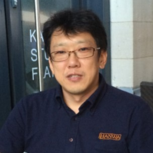
Masanori Sawada
Masanori Sawada was born in Wakayama, Japan, 1973. He received his M.S. from Wakayama University in March 1998. He joined Hanwa Electronic Ind. in April 1998. Currently, he is the president of HANWA ELECTRONIC IND.
2B.1 Consideration of Waveform Analysis and Test Method for Charged Board Event (RCJ Exchange Paper)
2B.2 Proposing a Strategy to Prevent Module-level Charged Device Model Failures in Dual In-line Memory Modules

Youngbong Han
Youngbong Han received his B.S. degree in 2015 and his M.S. and Ph.D degrees in 2020 from the College of Information and Communication Engineering, Sungkyunkwan University, Suwon, South Korea. Since 2020, he has been working on quality assurance tasks related to Electromagnetic Compatibility, Electrostatic Discharge, and Signal Integrity at Samsung Electronics' Device Solutions Quality Synergy P/J.
2B.2 Proposing a Strategy to Prevent Module-level Charged Device Model Failures in Dual In-line Memory Modules
Authors Corner for 2B.1 and 2B.2

Youngbong Han
Youngbong Han received his B.S. degree in 2015 and his M.S. and Ph.D degrees in 2020 from the College of Information and Communication Engineering, Sungkyunkwan University, Suwon, South Korea. Since 2020, he has been working on quality assurance tasks related to Electromagnetic Compatibility, Electrostatic Discharge, and Signal Integrity at Samsung Electronics' Device Solutions Quality Synergy P/J.

Masanori Sawada
Masanori Sawada was born in Wakayama, Japan, 1973. He received his M.S. from Wakayama University in March 1998. He joined Hanwa Electronic Ind. in April 1998. Currently, he is the president of HANWA ELECTRONIC IND.
Authors Corner for 2B.1 and 2B.2
2B.3 Intrinsic Inductance and Time-Dependent Resistance of the FI-CDM Spark

Timothy J. Maloney
Timothy J. Maloney graduated in physics and EE from MIT (SB 1971) and Cornell (MS 1973, PhD 1976). Following postdoctoral work at Cornell and semiconductor research at Varian Associates, Palo Alto, CA, he joined Intel Corp., Santa Clara, CA, in 1984, and has been concerned with IC ESD protection and testing, signal integrity, system ESD, and other topics. Dr. Maloney became a Senior Principal Engineer at Intel and retired in 2016. He has 40 patents, is co-author of a book, "Basic ESD and I/O Design" (Wiley, 1998), and is a Fellow of the IEEE. He has many publications at the EOS/ESD Symposium, IRPS, and other IEEE-connected entities.
2B.3 Intrinsic Inductance and Time-Dependent Resistance of the FI-CDM Spark
2B.4 The Demand for a CDM Bare Die Testing Method

Lena Zeitlhoefler
Lena Zeitlhöfler received her Master's degree in Electrical Engineering in 2017 from the Technical University of Munich (TUM). During her time as a Ph.D. student at the TUM, she worked in cooperation with Infineon Technologies AG in the fields of ESD and, particularly, on the physics of CDM and CDM simulation. She joined the ESD Team of Infineon in Munich, Germany, full-time in September 2021.
2B.4 The Demand for a CDM Bare Die Testing Method
2B.5 FI-CDM and LICCDM Testing on Wafer, Single Die, and Package Levels
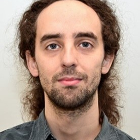
Marko Simicic
Marko Simicic received the M.Sc. degree in electrical engineering and information technology from the University of Zagreb, Croatia, in 2012. He obtained a PhD degree from the department of electrical engineering ESAT, KU Leuven, Belgium in 2018. Since 2017 he is an ESD researcher in imec, Belgium. He is a certified ESD control program manager since 2022. He has authored or co-authored more than 40 papers in international journals and conference proceedings. His current research area is rather wide and includes ESD device and circuit design in advanced semiconductor and 3D/2.5D stacking technologies, novel ESD testing and ESD control process assessment.
2B.5 FI-CDM and LICCDM Testing on Wafer, Single Die, and Package Levels
Authors Corner for 2B.3, 2B.4, and 2B.5

Timothy J. Maloney
Timothy J. Maloney graduated in physics and EE from MIT (SB 1971) and Cornell (MS 1973, PhD 1976). Following postdoctoral work at Cornell and semiconductor research at Varian Associates, Palo Alto, CA, he joined Intel Corp., Santa Clara, CA, in 1984, and has been concerned with IC ESD protection and testing, signal integrity, system ESD, and other topics. Dr. Maloney became a Senior Principal Engineer at Intel and retired in 2016. He has 40 patents, is co-author of a book, "Basic ESD and I/O Design" (Wiley, 1998), and is a Fellow of the IEEE. He has many publications at the EOS/ESD Symposium, IRPS, and other IEEE-connected entities.

Marko Simicic
Marko Simicic received the M.Sc. degree in electrical engineering and information technology from the University of Zagreb, Croatia, in 2012. He obtained a PhD degree from the department of electrical engineering ESAT, KU Leuven, Belgium in 2018. Since 2017 he is an ESD researcher in imec, Belgium. He is a certified ESD control program manager since 2022. He has authored or co-authored more than 40 papers in international journals and conference proceedings. His current research area is rather wide and includes ESD device and circuit design in advanced semiconductor and 3D/2.5D stacking technologies, novel ESD testing and ESD control process assessment.

Lena Zeitlhoefler
Lena Zeitlhöfler received her Master's degree in Electrical Engineering in 2017 from the Technical University of Munich (TUM). During her time as a Ph.D. student at the TUM, she worked in cooperation with Infineon Technologies AG in the fields of ESD and, particularly, on the physics of CDM and CDM simulation. She joined the ESD Team of Infineon in Munich, Germany, full-time in September 2021.
Authors Corner for 2B.3, 2B.4, and 2B.5
Wednesday, September 18
3B.1 A Statistical Explanation of CDM Qualification Variability

Theo Smedes
After receiving his Ph.D. from the Eindhoven University of Technology with a thesis on compact device modelling, Theo Smedes worked at the Delft University of Technology on layout-to-circuit extraction. In 1995 he joined NXP Semiconductors (Philips Semiconductors at that time), working on tools for statistical design. Currently, he is NXP Fellow for ESD and Latch-up. Theo is member of all ESDA device testing working groups and chairs the TLP working group. He published several papers on ESD and received the 2007 Best Paper Award and the 2009, 2018 and 2022 Outstanding Paper Award of the EOS/ESD Symposium. Theo was general chair of the EOS/ESD Symposium in 2013. He has been recognized with ESDA's David F. Barber Sr. Memorial Award (2017) and Outstanding Contribution Award (2022).
3B.1 A Statistical Explanation of CDM Qualification Variability
3B.2 Secondary Discharges during FICDM stress - Source and Solution
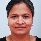
Sheela Verwoerd
Sheela Verwoerd received her M.Sc in Applied Physics in 2000 at the Indian Institute of Technology, Madras, India. She then moved to the Netherlands, where she did her PhD on "Full Chip Modelling of ICs under CDM stress" in the University of Twente in Enschede. She worked as ESD Assurance Engineer at Philips Semiconductors for a couple of years. After a brief gap of 10 years, she joined NXP Semiconductors as Principal ESD/LU test Engineer. She had been focused on ESD/LU qualification of ICs since then.
3B.2 Secondary Discharges during FICDM stress - Source and Solution
3B.3 System CDM Modeling for High-Speed Interface Devices

Emanuele Groppo
Emanuele Groppo received his B.Sc. (2020) and M.Sc. (2022) in Electronic Engineering from Politecnico di Torino, Italy. He is currently pursuing a Ph.D. at the Technical University of Munich (TUM), Chair of Circuit Design. In 2023, he joined the ESD team at Intel in Munich, Germany. The focus of his research is on novel ESD devices and solutions for advanced semiconductor technologies.
3B.3 System CDM Modeling for High-Speed Interface Devices
Authors Corner for 3B.1, 3B.2, and 3B.3

Emanuele Groppo
Emanuele Groppo received his B.Sc. (2020) and M.Sc. (2022) in Electronic Engineering from Politecnico di Torino, Italy. He is currently pursuing a Ph.D. at the Technical University of Munich (TUM), Chair of Circuit Design. In 2023, he joined the ESD team at Intel in Munich, Germany. The focus of his research is on novel ESD devices and solutions for advanced semiconductor technologies.

Theo Smedes
After receiving his Ph.D. from the Eindhoven University of Technology with a thesis on compact device modelling, Theo Smedes worked at the Delft University of Technology on layout-to-circuit extraction. In 1995 he joined NXP Semiconductors (Philips Semiconductors at that time), working on tools for statistical design. Currently, he is NXP Fellow for ESD and Latch-up. Theo is member of all ESDA device testing working groups and chairs the TLP working group. He published several papers on ESD and received the 2007 Best Paper Award and the 2009, 2018 and 2022 Outstanding Paper Award of the EOS/ESD Symposium. Theo was general chair of the EOS/ESD Symposium in 2013. He has been recognized with ESDA's David F. Barber Sr. Memorial Award (2017) and Outstanding Contribution Award (2022).

Sheela Verwoerd
Sheela Verwoerd received her M.Sc in Applied Physics in 2000 at the Indian Institute of Technology, Madras, India. She then moved to the Netherlands, where she did her PhD on "Full Chip Modelling of ICs under CDM stress" in the University of Twente in Enschede. She worked as ESD Assurance Engineer at Philips Semiconductors for a couple of years. After a brief gap of 10 years, she joined NXP Semiconductors as Principal ESD/LU test Engineer. She had been focused on ESD/LU qualification of ICs since then.