Monday, September 15
Opening Welcome
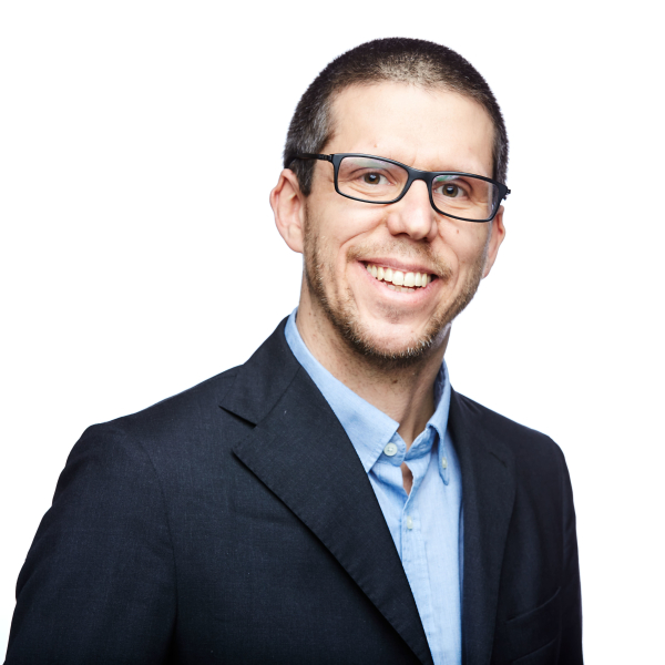
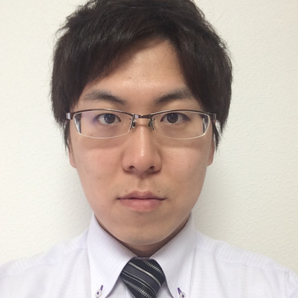
Mirko Scholz
In 2005, Dr. Mirko Scholz received his Diplom-Engineer (FH) degree in Electrical Engineering from the University of Applied Sciences in Zwickau, Germany. In 2013 Dr. Mirko Scholz received his PhD degree in Electrical Engineering from the Vrije Universiteit in Brussels (VUB), Belgium. From 2005 until 2017 he was working as an ESD researcher in different R&D programs at imec in Leuven/Belgium. From March 2017 until June 2019, he was a program manager in the imec academy and in imec’s process technology transfer activities.
Since July 2019 he has been with Infineon Technologies in Neubiberg, Germany where he is a Principal Engineer ESD Development. His daily work focuses on component- and system-level ESD protection design for RF, security, and automotive product lines at Infineon.
Since 2007 he has been an active member of different working groups in the ESD Association (ESDA) standards committee, currently co-chairing WG 5.6 (Human Metal Model). He was the management chair of the 2018 International ESD Workshop (IEW) in Belgium. Since 2019 he has been a member of the steering committee of the EOS/ESD Symposium. In this function he was the TPC chair in 2023 and the Vice Chair in 2024. He is the General Chair of the 2025 ESD Symposium.
For the 2017-2019 term and again for the 2022-2024 and 2025-2027 terms he has been an elected member of the ESDA Board of Directors. Since 2017 he is leading as a business unit manager the Advanced Topics committee of the ESDA.
He has authored/co-authored more than 100 publications, tutorials, and patents in the field of ESD protection design and testing. He is co-author of the 2014 Springer book “System-level ESD protection”. He is a regular reviewer for several IEEE journals and a current member of the IRPS sub-committee on ESD and Latchup.
Keynote: Small Wonders, Monumental Impact: The World of Semiconductor Innovation
Myung-Hee Na
Myung-Hee Na is currently the Vice President and Technology Systems General Manager in Intel, USA. Over 20 years, she has been known as the semiconductor technologist and held various executive positions in global semiconductor companies including US, Belgium and Korea. She has been very diverse and deep semiconductor experiences from device to designs including logic and memory technologies over 20 years. Prior to joining Intel in April 2024, over the past three years she was Vice President of the Revolutionary Technology Center in SK Hynix, Korea. In this role she was responsible for multi-decade semiconductor research roadmaps and strategies for memory centric and emerging computing domains such as emerging memory, and beyond memory.
From 2019-2023, Myung-Hee also worked at imec in Belgium where she was Vice President, Technology Solutions and Enablement. In this role she was responsible for overall 10-year research strategies for CMOS pathfinding and emerging computing domains such as edge computing. After completing her Ph.D. in Physics, Dr. Na started her career at IBM in 2001, where she held various technical, managerial and executive roles until early 2019. During that time, she was promoted to Distinguished Engineer and Technical Executive. At IBM Research, she successfully led Research and Development for multiple generations of semiconductor technologies, including high-K metal gate, FinFET, and Nanosheet development. Moreover, she has co-authored numerous research papers and U.S. and international patents.
ESDA Roadmap
1A.1 ESD Considerations for Photonics Products
Chloe Troussier
Chloe Troussier received her engineering degree in Embedded Systems and Electronics in 2018 from Institut Mines Telecom Atlantique in Brest, France, and her Ph.D degree in 2022 from the University of Grenoble Alpes, France. During her Ph.D. thesis, she studied the Charged device model phenomenon. Since 2022, she has been a member of the ESD team in Crolles, working on designing ESD protections.
1A.2 ESD HBM Failures of Different Cap Layer and Barrier Thinning Effects in GaN-on-Si AlGaN/GaN HEMTs
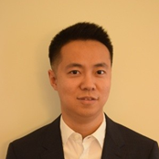
Wei-Min Wu
Wei-Min Wu received the dual Ph.D. degrees in electrical engineering from the KU Leuven, Belgium, and in electronic engineering from National Yang Ming Chiao Tung University (NYCU), Taiwan in 2022. He is now with IMEC, Leuven, Belgium as an RF ESD researcher. His current research interests include ESD protections in Design Technology Co-Optimization (DTCO) with the Si/III-V RF devices and circuits, and in high-speed I/O technology.
Authors Corner 1A.1 & 1A.2
Chloe Troussier
Chloe Troussier received her engineering degree in Embedded Systems and Electronics in 2018 from Institut Mines Telecom Atlantique in Brest, France, and her Ph.D degree in 2022 from the University of Grenoble Alpes, France. During her Ph.D. thesis, she studied the Charged device model phenomenon. Since 2022, she has been a member of the ESD team in Crolles, working on designing ESD protections.
Wei-Min Wu
Wei-Min Wu received the dual Ph.D. degrees in electrical engineering from the KU Leuven, Belgium, and in electronic engineering from National Yang Ming Chiao Tung University (NYCU), Taiwan in 2022. He is now with IMEC, Leuven, Belgium as an RF ESD researcher. His current research interests include ESD protections in Design Technology Co-Optimization (DTCO) with the Si/III-V RF devices and circuits, and in high-speed I/O technology.
Presentation and Interactive Workshop - System Level Direct Pin ESD – The White Elephant in the Room for System ESD Testing
Harald Gossner
Harald Gossner (Senior Member, IEEE) received the Dipl.-Phys. degree from Ludwig-Maximilian's University, Munich, Germany, in 1990, and the Ph.D. degree in electrical engineering from University der Bundeswehr, Munich, Germany, in 1995. He is currently a Senior Principal Engineer with Intel, Neubiberg, Germany. Dr. Gossner is a Co-Founder and Co-Chair of the Industry Council on ESD Target Levels.
Invited Talk - Statistical Characterization of Human-Induced ESD for Field Risk Assessment
Satyajeet Shinde
2A.1 Transient Response of Very Fast Transmission Line Pulse: Procedures for Measurement Verification
Leonardo Di Biccari
Leonardo Di Biccari graduated (summa cum laude) in electronic engineering at the University of Padova. He is a member of the Technical Staff at STMicroelectronics, where he is leading the group responsible for ESD protection development in BCD technologies. Since 2012, Leonardo has been representing STMicroelectronics in the main ESDA standardization committees, including HBM, CDM, and TLP, where he is currently acting as vice-chair. Since 2024, he has been serving in the ESDA Standard Committee. Leonardo authored several papers on ESD and EDA topics presented at ESREF, IRPS, and the EOS/ESD Symposium, where he regularly served in the Technical Program Committee.
2A.2 Statistical Analysis of (VF-)TLP Parameter Variability
Theo Smedes
After receiving his Ph.D. from the Eindhoven University of Technology with a thesis on compact device modelling, Theo Smedes worked at the Delft University of Technology on layout-to-circuit extraction. In 1995, he joined NXP Semiconductors (Philips Semiconductors at that time), working on tools for statistical design. Currently, he is an NXP Fellow for ESD and Latch-up. Theo is a member of all ESDA device testing working groups and chairs the TLP working group. He published several papers on ESD and received the 2007 Best Paper Award and the 2009, 2018, and 2022 Outstanding Paper Award of the EOS/ESD Symposium. Theo was the general chair of the EOS/ESD Symposium in 2013. He has been recognized with ESDA's David F. Barber Sr. Memorial Award (2017) and Outstanding Contribution Award (2022).
2A.3 AI-Driven Analysis of VF-TLP and TLP Characteristics via Hierarchical Clustering
Seyed Hossein Hosseini
2A.1, 2A.2, & 2A.3 Authors Corner
Leonardo Di Biccari
Leonardo Di Biccari graduated (summa cum laude) in electronic engineering at the University of Padova. He is a member of the Technical Staff at STMicroelectronics, where he is leading the group responsible for ESD protection development in BCD technologies. Since 2012, Leonardo has been representing STMicroelectronics in the main ESDA standardization committees, including HBM, CDM, and TLP, where he is currently acting as vice-chair. Since 2024, he has been serving in the ESDA Standard Committee. Leonardo authored several papers on ESD and EDA topics presented at ESREF, IRPS, and the EOS/ESD Symposium, where he regularly served in the Technical Program Committee.
Seyed Hossein Hosseini
Theo Smedes
After receiving his Ph.D. from the Eindhoven University of Technology with a thesis on compact device modelling, Theo Smedes worked at the Delft University of Technology on layout-to-circuit extraction. In 1995, he joined NXP Semiconductors (Philips Semiconductors at that time), working on tools for statistical design. Currently, he is an NXP Fellow for ESD and Latch-up. Theo is a member of all ESDA device testing working groups and chairs the TLP working group. He published several papers on ESD and received the 2007 Best Paper Award and the 2009, 2018, and 2022 Outstanding Paper Award of the EOS/ESD Symposium. Theo was the general chair of the EOS/ESD Symposium in 2013. He has been recognized with ESDA's David F. Barber Sr. Memorial Award (2017) and Outstanding Contribution Award (2022).
Tuesday, September 16
Morning Welcome
Mirko Scholz
In 2005, Dr. Mirko Scholz received his Diplom-Engineer (FH) degree in Electrical Engineering from the University of Applied Sciences in Zwickau, Germany. In 2013 Dr. Mirko Scholz received his PhD degree in Electrical Engineering from the Vrije Universiteit in Brussels (VUB), Belgium. From 2005 until 2017 he was working as an ESD researcher in different R&D programs at imec in Leuven/Belgium. From March 2017 until June 2019, he was a program manager in the imec academy and in imec’s process technology transfer activities.
Since July 2019 he has been with Infineon Technologies in Neubiberg, Germany where he is a Principal Engineer ESD Development. His daily work focuses on component- and system-level ESD protection design for RF, security, and automotive product lines at Infineon.
Since 2007 he has been an active member of different working groups in the ESD Association (ESDA) standards committee, currently co-chairing WG 5.6 (Human Metal Model). He was the management chair of the 2018 International ESD Workshop (IEW) in Belgium. Since 2019 he has been a member of the steering committee of the EOS/ESD Symposium. In this function he was the TPC chair in 2023 and the Vice Chair in 2024. He is the General Chair of the 2025 ESD Symposium.
For the 2017-2019 term and again for the 2022-2024 and 2025-2027 terms he has been an elected member of the ESDA Board of Directors. Since 2017 he is leading as a business unit manager the Advanced Topics committee of the ESDA.
He has authored/co-authored more than 100 publications, tutorials, and patents in the field of ESD protection design and testing. He is co-author of the 2014 Springer book “System-level ESD protection”. He is a regular reviewer for several IEEE journals and a current member of the IRPS sub-committee on ESD and Latchup.
GaN Devices: Technology, Reliability-Limiting Processes and ESD Failures
Matteo Meneghini
Matteo Meneghini received his PhD (University of Padova) working on the optimization of GaN-based LED and laser structures.
He is now a full professor at the Department of Information Engineering at the University of Padova. His main interests are the characterization, reliability, and modeling of compound semiconductor devices (LEDs, laser diodes, HEMTs) and optoelectronic components, including solar cells. He has published more than 400 journal and conference proceedings papers related to these activities.
During his career, he has cooperated and/or co-published with several semiconductor companies and research centers. He has been elected IEEE Fellow (Class of 2025). He and his colleagues have won several best paper awards at international conferences.
3A.1 Innovative ESD Protection for RF Circuits: Integrating Diodes into Capacitors in Advanced Technology
Thalis Da Costa Guedes
Thalis da Costa Guedes received his bachelor's degree in electrical engineering from "Universidade Federal de Campina Grande" and his M.Sc. degree in electronics systems from "Institut National Polytechnique de Grenoble" (INPG) through the prestigious Eiffel double degree program in 2023. Currently, he is pursuing a Ph.D. in micro and nanoelectronics at "Université Grenoble Alpes" in partnership with STMicroelectronics. He is dedicated to researching and developing solutions for electrostatic discharge protection in radiofrequency circuits, with articles and patents in the field.
3A.2 Low-C ESD Protection Design With Improved BEOL Layout Style for High-Frequency Applications
Chen-Yu Liang
Chen-Yu Liang received the B.S. degree from the Department of Physics from National Tsing-Hua University (NTHU), Hsinchu, Taiwan, R.O.C., in 2015 and the M.S. degree from the Institute of Electronics, National Chiao-Tung University (NCTU), Hsinchu, Taiwan, R.O.C., in 2019. He is currently working toward the Ph.D. degree at the Institute of Electronics, National Yang Ming Chiao Tung University (NYCU), Hsinchu, Taiwan. His current research interests include high-speed I/O circuits and ESD protection design for mixed-signal and RF ICs.
3A.3 CDM Protection of an Antenna Pad in CMOS Technology
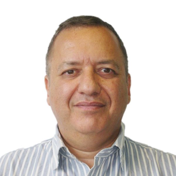
Michael Stockinger
Michael Stockinger (PhD, 2000, Vienna University, Austria) is Technical Director at NXP's Advanced Chip Engineering division, Austin, Texas, focusing on ESD and LU. His design solutions have been implemented in Kinetis, i.MX, ColdFire, and MCX product lines. Michael received ESD Symposium Best Paper or Best Presentation awards in 2001, 2003, 2013, and 2020 and the Industry Pioneer Recognition Award in 2023. He has over 40 papers and 33 patents. He served on TPCs of the ESD Symposium and the IRPS and teaches tutorials and online courses. Michael is chair of the JESD78 workgroup and Si2's CMC ASM-ESD diode model workgroup.
3A.1, 3A.2, & 3A.3 Authors Corner
Thalis Da Costa Guedes
Thalis da Costa Guedes received his bachelor's degree in electrical engineering from "Universidade Federal de Campina Grande" and his M.Sc. degree in electronics systems from "Institut National Polytechnique de Grenoble" (INPG) through the prestigious Eiffel double degree program in 2023. Currently, he is pursuing a Ph.D. in micro and nanoelectronics at "Université Grenoble Alpes" in partnership with STMicroelectronics. He is dedicated to researching and developing solutions for electrostatic discharge protection in radiofrequency circuits, with articles and patents in the field.
Chen-Yu Liang
Chen-Yu Liang received the B.S. degree from the Department of Physics from National Tsing-Hua University (NTHU), Hsinchu, Taiwan, R.O.C., in 2015 and the M.S. degree from the Institute of Electronics, National Chiao-Tung University (NCTU), Hsinchu, Taiwan, R.O.C., in 2019. He is currently working toward the Ph.D. degree at the Institute of Electronics, National Yang Ming Chiao Tung University (NYCU), Hsinchu, Taiwan. His current research interests include high-speed I/O circuits and ESD protection design for mixed-signal and RF ICs.
Michael Stockinger
Michael Stockinger (PhD, 2000, Vienna University, Austria) is Technical Director at NXP's Advanced Chip Engineering division, Austin, Texas, focusing on ESD and LU. His design solutions have been implemented in Kinetis, i.MX, ColdFire, and MCX product lines. Michael received ESD Symposium Best Paper or Best Presentation awards in 2001, 2003, 2013, and 2020 and the Industry Pioneer Recognition Award in 2023. He has over 40 papers and 33 patents. He served on TPCs of the ESD Symposium and the IRPS and teaches tutorials and online courses. Michael is chair of the JESD78 workgroup and Si2's CMC ASM-ESD diode model workgroup.
System Level Workshop - Steps Towards the Root Cause
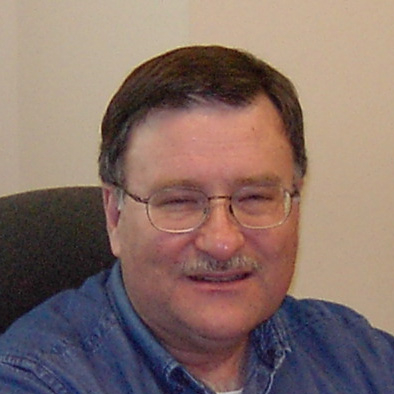
Steffen Holland
Steffen Holland received his diploma and PhD in Physics from the University of Hamburg in 2004. He joined Philips Semiconductors/NXP/Nexperia in the process development group for discrete bipolar devices in Hamburg, Germany in 2005. The main focus of his work quickly became TCAD process and device simulations for discrete ESD protection devices. He works now on discrete ESD protection devices. His current interests are system level ESD simulations. He currently serves in the Board of Directors at the ESD Association and is chair of the ESDA working group 26.
Shubhankar Marathe
Keynote: Induction: An Invisible Menace
David E. Swenson
David E. Swenson retired in 2003 after 35 years of service from 3M. While at 3M he had responsibility for new packaging material development and application, training of 3M personnel worldwide and providing application assistance to users of static control products globally with particular emphasis on Asia Pacific and Japan. Dave and his wife Geri established a new company, Affinity Static Control Consulting, L.L.C .in 2003. Dave has been a member of the ESD Association since 1984 and has served in many capacities including 1997 Symposium General Chair and president of the Association in 1998 and 1999 and again in 2008 and 2009. He was re-elected to the Board of Directors for a 5th term from 2014 to 2016 and is currently appointed to the Board to assist with technical inquiries. Dave was presented with the highest award of the ESD Association, the “Outstanding Contributions Award” in 2002, the Standards Committee “Joel P. Weidendorf Memorial Award” in 2004, the Association “Edward G. Weggeland” Memorial Award in 2014 and the Symposium Committee’s, David Barber, Sr. Memorial award in 2018. He is a member of the Standards Committee serving several Working Groups and the ANSI/ESD S20.20 Standard Task Team. Dave also serves as Treasurer and Information Liaison of the Texas Chapter of the ESD Association; he is a member of the Electrostatic Society of America, IMAPS, the UK Institute of Physics and is a US Expert to IEC TC101, Electrostatics.
4A.1 ESD Air Discharges into Shielded Automotive RF Connectors

Martin Pilaski
Martin Pilaski holds a diploma in Computer Engineering from Mannheim University. He joined Philips Semiconductors in 2005 and has since then worked in several product design and application marketing roles for NXP and Nexperia. Martin is currently responsible for worldwide product application support of Nexperia's Bipolar Discretes portfolio with a focus on ESD and EMC for mobile, portable, consumer, and computing applications.
4A.2 Radial Transmission Line Effects in Charged Device Model Events and Testing
Timothy J. Maloney
Timothy J. Maloney graduated in physics and EE from MIT (SB 1971) and Cornell (MS 1973, PhD 1976). Following postdoctoral work at Cornell and semiconductor research at Varian Associates, Palo Alto, CA, he joined Intel Corp., Santa Clara, CA, in 1984, and has been concerned with IC ESD protection and testing, signal integrity, system ESD, and other topics. Dr. Maloney became a Senior Principal Engineer at Intel and retired in 2016. He has 40 patents, is co-author of a book, "Basic ESD and I/O Design" (Wiley, 1998), and is a Fellow of the IEEE. He has many publications at the EOS/ESD Symposium, IRPS, and other IEEE-connected entities.
4A.3 Effect of Pulse Duration in Transient Latchup Events
Guido Quax
Guido Quax received an MSc and Ph.D. in Applied Physics at the Eindhoven University of Technology in 2003 and 2008, respectively. His Ph.D. research focused on the electrical and optical properties of III-V semiconductor quantum dots. After graduation, he worked in the field of optical properties of soft matter at Philips Research. He joined the ESD team of NXP Semiconductors in 2012, focusing on high voltage and power applications. He has an interest in the experiments and modeling of parasitic bipolars and thyristors in Silicon.
4A.4 Degradation of PN-Junction Devices Subjected to Multiple Surge Pulses
Steffen Holland
Steffen Holland received his diploma and PhD in Physics from the University of Hamburg in 2004. He joined Philips Semiconductors/NXP/Nexperia in the process development group for discrete bipolar devices in Hamburg, Germany in 2005. The main focus of his work quickly became TCAD process and device simulations for discrete ESD protection devices. He works now on discrete ESD protection devices. His current interests are system level ESD simulations. He currently serves in the Board of Directors at the ESD Association and is chair of the ESDA working group 26.
4A.1, 4A.2, 4A.3, & 4A.4 Authors Corner
Steffen Holland
Steffen Holland received his diploma and PhD in Physics from the University of Hamburg in 2004. He joined Philips Semiconductors/NXP/Nexperia in the process development group for discrete bipolar devices in Hamburg, Germany in 2005. The main focus of his work quickly became TCAD process and device simulations for discrete ESD protection devices. He works now on discrete ESD protection devices. His current interests are system level ESD simulations. He currently serves in the Board of Directors at the ESD Association and is chair of the ESDA working group 26.
Timothy J. Maloney
Timothy J. Maloney graduated in physics and EE from MIT (SB 1971) and Cornell (MS 1973, PhD 1976). Following postdoctoral work at Cornell and semiconductor research at Varian Associates, Palo Alto, CA, he joined Intel Corp., Santa Clara, CA, in 1984, and has been concerned with IC ESD protection and testing, signal integrity, system ESD, and other topics. Dr. Maloney became a Senior Principal Engineer at Intel and retired in 2016. He has 40 patents, is co-author of a book, "Basic ESD and I/O Design" (Wiley, 1998), and is a Fellow of the IEEE. He has many publications at the EOS/ESD Symposium, IRPS, and other IEEE-connected entities.
Martin Pilaski
Martin Pilaski holds a diploma in Computer Engineering from Mannheim University. He joined Philips Semiconductors in 2005 and has since then worked in several product design and application marketing roles for NXP and Nexperia. Martin is currently responsible for worldwide product application support of Nexperia's Bipolar Discretes portfolio with a focus on ESD and EMC for mobile, portable, consumer, and computing applications.
Guido Quax
Guido Quax received an MSc and Ph.D. in Applied Physics at the Eindhoven University of Technology in 2003 and 2008, respectively. His Ph.D. research focused on the electrical and optical properties of III-V semiconductor quantum dots. After graduation, he worked in the field of optical properties of soft matter at Philips Research. He joined the ESD team of NXP Semiconductors in 2012, focusing on high voltage and power applications. He has an interest in the experiments and modeling of parasitic bipolars and thyristors in Silicon.
Wednesday, September 17
Morning Welcome
Mirko Scholz
In 2005, Dr. Mirko Scholz received his Diplom-Engineer (FH) degree in Electrical Engineering from the University of Applied Sciences in Zwickau, Germany. In 2013 Dr. Mirko Scholz received his PhD degree in Electrical Engineering from the Vrije Universiteit in Brussels (VUB), Belgium. From 2005 until 2017 he was working as an ESD researcher in different R&D programs at imec in Leuven/Belgium. From March 2017 until June 2019, he was a program manager in the imec academy and in imec’s process technology transfer activities.
Since July 2019 he has been with Infineon Technologies in Neubiberg, Germany where he is a Principal Engineer ESD Development. His daily work focuses on component- and system-level ESD protection design for RF, security, and automotive product lines at Infineon.
Since 2007 he has been an active member of different working groups in the ESD Association (ESDA) standards committee, currently co-chairing WG 5.6 (Human Metal Model). He was the management chair of the 2018 International ESD Workshop (IEW) in Belgium. Since 2019 he has been a member of the steering committee of the EOS/ESD Symposium. In this function he was the TPC chair in 2023 and the Vice Chair in 2024. He is the General Chair of the 2025 ESD Symposium.
For the 2017-2019 term and again for the 2022-2024 and 2025-2027 terms he has been an elected member of the ESDA Board of Directors. Since 2017 he is leading as a business unit manager the Advanced Topics committee of the ESDA.
He has authored/co-authored more than 100 publications, tutorials, and patents in the field of ESD protection design and testing. He is co-author of the 2014 Springer book “System-level ESD protection”. He is a regular reviewer for several IEEE journals and a current member of the IRPS sub-committee on ESD and Latchup.
Keynote: Backside Interconnects for Future Advanced Nodes
Ruilong Xie
Ruilong Xie (Senior Member, IEEE) received his Bachelor of Engineering degree in 2006 and Ph.D. degree in 2010 in Electrical and Computer Engineering from the National University of Singapore (NUS). During his Ph.D., he worked in the Silicon Nano Device Laboratory at NUS and was associated with the Institute of Microelectronics, Agency for Science, Technology and Research, Singapore. His doctoral research focused on high-mobility germanium channel MOSFETs with high-k gate dielectrics. In 2009, Ruilong joined Chartered Semiconductor Manufacturing in Singapore, where he contributed to the development of 45nm and 55nm CMOS technologies. He later moved to the GLOBALFOUNDRIES Research division in Albany, NY, working on advanced FinFET technologies (14nm, 10nm, and 7nm FinFET nodes) as part of the IBM Technology Development Alliances. Since 2018, Ruilong has been with IBM Research, focusing on advanced technology nodes, including nanosheet transistors, vertical transistors, and backside interconnect technologies. He holds more than 1,000 U.S. patents and has authored or co-authored over 30 conference and journal papers.
5A.1 Metal Electrothermal Model for Circuit Simulation
Eugene Worley
Eugene Worley received an MSEE degree from the University of California at Berkeley in solid state electronics. His career has included IC circuit design, semiconductor device characterization, and reliability physics. He is presently a consulting engineer with Silicon Crossing, LLC. For over 10 years he has worked on the design and characterization of ESD clamps for LNA's, RF power amplifiers, power management circuits, analog circuits, low capacitance SERDES clamps, and advanced digital circuits for Qualcomm as a principal engineer. His ESDA activities include being a member of the TLP working group, workshop moderator, workshop panelist for six years, session chair for five years, technical program committee member for over 14 years, and IEW seminar chair. He has published papers in the IEEE Transactions on Electron Devices, IEEE Electron Device Letters, IEEE J. of Solid State Circuits, Solid State Electronics, the Technical Digest of the International Electron Devices Meeting, the EOS/ESD Symposium Proceedings, Journal of Electrostatics, and the IEEE Transactions on Nuclear Science. He has also reviewed papers for the IEEE Transactions on Electron Devices, the Journal of Electrostatics, and the IEEE Transactions on Device and Materials Reliability. He is a member of Tau Beta Pi, Eta Kappa Nu, and Phi Kappa Phi.
5A.2 Empirical ESD Modeling of ESD Pass Gate Transistors
Efraim Aharoni
Efraim Aharoni received the M.Sc. and Ph.D degrees in Physics in 1989 and 1994 from the Technion, Israel Institute of Technology. His research in the Technion was focused on High Temperature Superconducting devices. In 1993 he joined Tower Semiconductor. Efraim worked in Tower in a variety of fields, in both engineering and management, in development as well as production. Amongst his engineering roles: process, device, yield, director R&D CMOS, and director of reliability. In the past 15 years, he has led the ESD and Latch-Up activities in the company as a senior principal engineer. This involves the development of new ESD devices and protection concepts, creating libraries of ESD devices in PDK, development of a unique concept of ‘empirical ESD modeling (for simulation of circuits containing snap-back based devices), PERC, and customer support. He works closely with the Tower design center, device engineers, PDK group, customers, and production lines, in Tower Semiconductor sites worldwide. Efraim served in the technical committees of IEW and EOS/ESD symposium, is a co-chair of WG22, and a member in the Industry Council of ESD Standards. In addition, he serves as the head of the Electrical Engineering department in the Kinneret College on the sea of Galilee and lectures on a variety of courses.
5A.3 Corona Discharge to Touchscreen Modeling Using Nonlinear Time-dependent Corona Streamer Propagation Model in SPICE
Zhekun Peng
6A.1 ESD Power Clamp Using Variable Clamping Voltage for Enhanced ESD Robustness and Prevention of False Triggering in High Voltage Applications
Kazuki Shimada
Kazuki Shimada received the B.E. degree in electrical engineering from the University of Toyama prefectural, Japan, in 2010. He currently works at Renesas Electronics Corporation as a System-level ESD and EMS design engineer. He mainly ESD and EMS design and troubleshoot for high voltage analog BCD and flash embedded MCU products.
6A.2 Area-Efficient and Low-Leakage Design for GaN-on-Si Power-Rail ESD Clamp Circuit With D-HEMT
Chao-Yang Ke
Chao-Yang Ke received the B.S. degree from the Department of Electronics Engineering, Chang Gung University, Taoyuan, Taiwan, in 2017, and the M.S. degree from the Institute of Electronics, National Chiao Tung University, in 2020. After graduating from the master's program, he joined the High Voltage ESD Program, R&D Department, TSMC, Hsinchu, as an ESD design engineer in 2020. He is currently pursuing the Ph.D. degree in the Institute of Electronics, National Yang Ming Chiao Tung University, Hsinchu, Taiwan. His current research interests include ESD design, latchup prevention, and safe operating area design in wide-bandgap semiconductor integrated circuits.
6A.1 & 6A.2 Authors Corner
Chao-Yang Ke
Chao-Yang Ke received the B.S. degree from the Department of Electronics Engineering, Chang Gung University, Taoyuan, Taiwan, in 2017, and the M.S. degree from the Institute of Electronics, National Chiao Tung University, in 2020. After graduating from the master's program, he joined the High Voltage ESD Program, R&D Department, TSMC, Hsinchu, as an ESD design engineer in 2020. He is currently pursuing the Ph.D. degree in the Institute of Electronics, National Yang Ming Chiao Tung University, Hsinchu, Taiwan. His current research interests include ESD design, latchup prevention, and safe operating area design in wide-bandgap semiconductor integrated circuits.
Kazuki Shimada
Kazuki Shimada received the B.E. degree in electrical engineering from the University of Toyama prefectural, Japan, in 2010. He currently works at Renesas Electronics Corporation as a System-level ESD and EMS design engineer. He mainly ESD and EMS design and troubleshoot for high voltage analog BCD and flash embedded MCU products.
Circuit Design Workshop: ESD Model Standards
Meng Miao
Michael Stockinger
Michael Stockinger (PhD, 2000, Vienna University, Austria) is Technical Director at NXP's Advanced Chip Engineering division, Austin, Texas, focusing on ESD and LU. His design solutions have been implemented in Kinetis, i.MX, ColdFire, and MCX product lines. Michael received ESD Symposium Best Paper or Best Presentation awards in 2001, 2003, 2013, and 2020 and the Industry Pioneer Recognition Award in 2023. He has over 40 papers and 33 patents. He served on TPCs of the ESD Symposium and the IRPS and teaches tutorials and online courses. Michael is chair of the JESD78 workgroup and Si2's CMC ASM-ESD diode model workgroup.
7A.1 Transient Simulation of CDM Currents in a Multichip Module Based on Measurements and 3D FEM Simulations
Ellen Merkel
Ellen Merkel joined the Analysis & Test group at Fraunhofer EMFT in 2018 and has been supporting the team in researching topics related to electrostatic discharges. She received her Bachelor's (2018) and Master's degree (2021) at the Technical University of Munich (TUM), Germany. Since then, she has worked as a research associate at Fraunhofer EMFT, specializing in ESD test methods, ESD robustness and protection, and simulations. In 2022, she started to work on her PhD with a focus on ESD risks in Multi-Chip Modules (MCM) and Systems in Package (SiP). Ellen is an active member of the ESD Association and joined the steering committee of the International ESD Workshop 2023 in Tutzing, Germany.
7A.2 ESD EDA Verification Evolution for Packages and Modules
Michael Khazhinsky
Michael G. Khazhinsky is currently a Principal ESD engineer/designer at Silicon Labs in Austin, Texas. Prior to joining Silicon Labs, he worked at Motorola and Freescale Semiconductors where he was in charge of the TCAD development and ESD/latch-up protection solutions for emerging process technologies, with a focus on ESD-EDA. Michael has M.S.E.E. and M.S. Physics from the Moscow State Institute of Electronic Engineering, and Ph.D. in Physics from Western Michigan University. Michael is the Chair of ESDA Working Group 18 on EDA. Michael has served as a member of the IRPS, IEW, ESREF, EMC and EOS/ESD Symposium Technical Program Committees, as well as a Workshop Chair, Technical Program Chair, Vice General Chair and General Chair of EOS/ESD Symposium. He currently serves on the Technical Program Committees of 2019 International Reliability Physics Symposium, 2019 EMC Symposium, 2019 ESREF and 2019 EOS/ESD Symposium. Michael co-authored over 30 papers and gave a number of invited talks on ESD, EDA, process/device TCAD, and photonic crystals. He was a co-recipient of seven EOS/ESD Symposium and SOI Symposium “Best Paper” and “Best Presentation” awards. Michael currently holds eighteen patents on ESD design, with additional patents pending. Michael is a Senior Member of IEEE and the Director of the ESD Association.
7A.3 Ultrafast Characterization of Gated and STI Diodes in Bulk FinFET and GAAFET Technologies
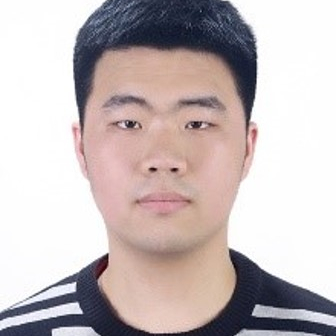
Emanuele Groppo
Emanuele Groppo received his B.Sc. (2020) and M.Sc. (2022) in Electronic Engineering from Politecnico di Torino, Italy. He is currently pursuing a Ph.D. at the Technical University of Munich (TUM), Chair of Circuit Design. In 2023, he joined the ESD team at Intel in Munich, Germany. The focus of his research is on novel ESD devices and solutions for advanced semiconductor technologies.
7A.4 Charge Trapping Mechanism in Thick Oxide of HV LDMOS Under CDM Events
Leonardo Di Biccari
Leonardo Di Biccari graduated (summa cum laude) in electronic engineering at the University of Padova. He is a member of the Technical Staff at STMicroelectronics, where he is leading the group responsible for ESD protection development in BCD technologies. Since 2012, Leonardo has been representing STMicroelectronics in the main ESDA standardization committees, including HBM, CDM, and TLP, where he is currently acting as vice-chair. Since 2024, he has been serving in the ESDA Standard Committee. Leonardo authored several papers on ESD and EDA topics presented at ESREF, IRPS, and the EOS/ESD Symposium, where he regularly served in the Technical Program Committee.
7A.1, 7A.2, 7A.3, & 7A.4 Authors Corner
Leonardo Di Biccari
Leonardo Di Biccari graduated (summa cum laude) in electronic engineering at the University of Padova. He is a member of the Technical Staff at STMicroelectronics, where he is leading the group responsible for ESD protection development in BCD technologies. Since 2012, Leonardo has been representing STMicroelectronics in the main ESDA standardization committees, including HBM, CDM, and TLP, where he is currently acting as vice-chair. Since 2024, he has been serving in the ESDA Standard Committee. Leonardo authored several papers on ESD and EDA topics presented at ESREF, IRPS, and the EOS/ESD Symposium, where he regularly served in the Technical Program Committee.
Emanuele Groppo
Emanuele Groppo received his B.Sc. (2020) and M.Sc. (2022) in Electronic Engineering from Politecnico di Torino, Italy. He is currently pursuing a Ph.D. at the Technical University of Munich (TUM), Chair of Circuit Design. In 2023, he joined the ESD team at Intel in Munich, Germany. The focus of his research is on novel ESD devices and solutions for advanced semiconductor technologies.
Michael Khazhinsky
Michael G. Khazhinsky is currently a Principal ESD engineer/designer at Silicon Labs in Austin, Texas. Prior to joining Silicon Labs, he worked at Motorola and Freescale Semiconductors where he was in charge of the TCAD development and ESD/latch-up protection solutions for emerging process technologies, with a focus on ESD-EDA. Michael has M.S.E.E. and M.S. Physics from the Moscow State Institute of Electronic Engineering, and Ph.D. in Physics from Western Michigan University. Michael is the Chair of ESDA Working Group 18 on EDA. Michael has served as a member of the IRPS, IEW, ESREF, EMC and EOS/ESD Symposium Technical Program Committees, as well as a Workshop Chair, Technical Program Chair, Vice General Chair and General Chair of EOS/ESD Symposium. He currently serves on the Technical Program Committees of 2019 International Reliability Physics Symposium, 2019 EMC Symposium, 2019 ESREF and 2019 EOS/ESD Symposium. Michael co-authored over 30 papers and gave a number of invited talks on ESD, EDA, process/device TCAD, and photonic crystals. He was a co-recipient of seven EOS/ESD Symposium and SOI Symposium “Best Paper” and “Best Presentation” awards. Michael currently holds eighteen patents on ESD design, with additional patents pending. Michael is a Senior Member of IEEE and the Director of the ESD Association.
Ellen Merkel
Ellen Merkel joined the Analysis & Test group at Fraunhofer EMFT in 2018 and has been supporting the team in researching topics related to electrostatic discharges. She received her Bachelor's (2018) and Master's degree (2021) at the Technical University of Munich (TUM), Germany. Since then, she has worked as a research associate at Fraunhofer EMFT, specializing in ESD test methods, ESD robustness and protection, and simulations. In 2022, she started to work on her PhD with a focus on ESD risks in Multi-Chip Modules (MCM) and Systems in Package (SiP). Ellen is an active member of the ESD Association and joined the steering committee of the International ESD Workshop 2023 in Tutzing, Germany.